Chiplet Summit 2026 · Technical Talk
Designing Chiplets to Accelerate AI:
The 10GW Challenge
How chiplet architecture, power delivery, and near-memory compute are the engineers' answer to AI's insatiable energy appetite
Author: Dr. Jawad Nasrullah, Affiliation: Palo Alto Electron Inc., Presented: February 18, 2026, Forum: Chiplet Summit 2026
AI datacenters are on track to consume 10 gigawatts of power. The only viable path forward isn't bigger power plants — it's smarter chips. Dr. Jawad Nasrullah lays out the four chiplet design moves that can cut AI energy consumption by an order of magnitude: node mixing, vertical power delivery, low-swing D2D links, and near-memory compute. This is the hardware engineer's roadmap to sustainable AI.
The scale of AI infrastructure is now measured in gigawatts. As large language models grow and inference demand accelerates, the semiconductor industry faces a compounding challenge that no single technology can solve alone. At Chiplet Summit 2026, Dr. Jawad Nasrullah of Palo Alto Electron Inc presented a rigorous framework for how chiplet-based architectures can address what he calls "the 10GW challenge" — the looming energy crisis at the heart of AI hardware.
This article reconstructs the talk's key arguments and technical toolkit, with original slides embedded throughout.
The Walls AI Hardware Must Break Through
AI systems today are not compute-bound — they are wall-bound. Nasrullah identifies three converging constraints that hardware designers must address simultaneously:
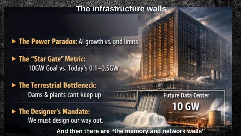
Slide 3: The three structural bottlenecks constrain AI infrastructure scaling.
The Three Walls
Memory wall: AI inference (particularly decode) is memory-bandwidth-bound. Systems are starved for data, not compute cycles.
Network wall: User experience demands low-latency interconnect. Multi-chip systems introduce coordination overhead that penalizes response time.
Power wall: Energy efficiency directly determines the cost per AI token — and at scale, this defines economic viability.
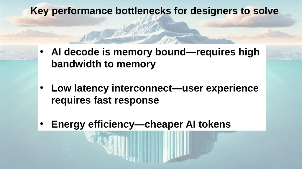
Slide 4: The three performance bottlenecks designers must solve: memory bandwidth, interconnect latency, and energy efficiency.
The Full Efficiency Stack: Where Gains Come From
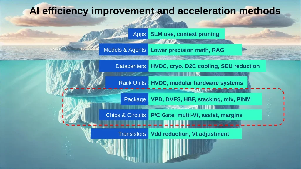
Slide 5: Efficiency improvements span every level of the stack, from applications and models down to transistors.
Efficiency improvements span every level of the stack, from applications and models down to transistors.
One of the talk's most useful contributions is its taxonomy of efficiency improvements across the entire hardware stack. Nasrullah maps techniques from the application layer — small language model use, context pruning — all the way down to transistor-level Vdd reduction. The implication is that no single optimization is sufficient; sustainable AI hardware requires coordinated improvements at every layer.
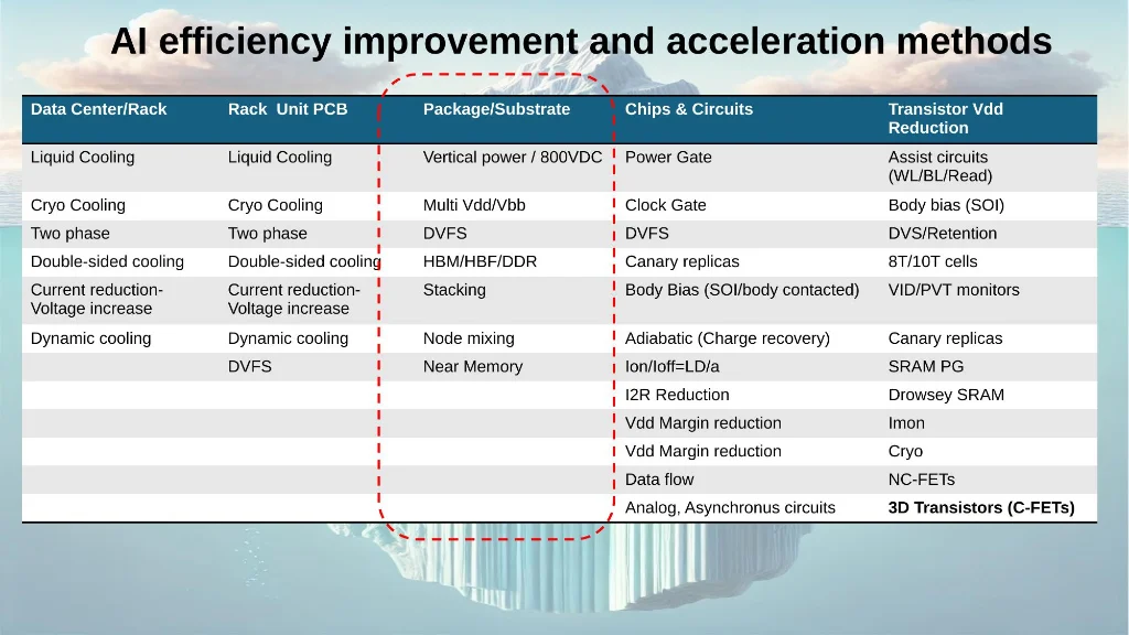
Slide 7: Comprehensive breakdown of efficiency techniques from datacenter cooling down to transistor physics.
Key insight: The efficiency improvement toolkit is deep at every level of abstraction. The biggest wins, however, come from architectural decisions made at the package and chiplet level — where the greatest design freedom still exists.
Four Chiplet-Level Techniques That Move the Needle
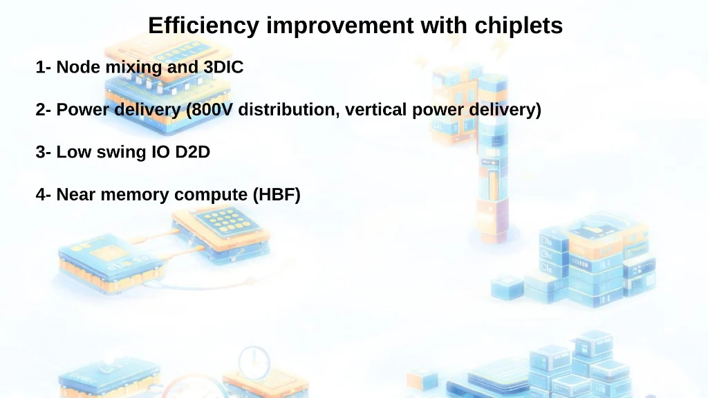
Slide 8: The four primary areas where chiplet architecture can drive efficiency gains.
The core of the talk focuses on four specific chiplet design techniques that, together, can dramatically reduce the energy footprint of AI accelerator systems.
1. Node Mixing and 3D-IC
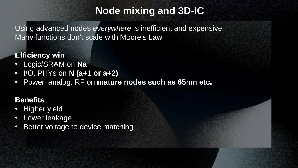
Slide 9: The case for node mixing — using leading-edge silicon only where it actually pays off.
The premise of node mixing is deceptively simple: not every function benefits from the latest process node. Advanced nodes are expensive, power-hungry for certain workloads, and wasteful when applied to I/O, analog, or RF functions that don't scale with Moore's Law.
The optimal chiplet-based approach allocates process nodes by function:
Node Allocation Strategy
Logic and SRAM → latest node (Na): Compute density and leakage reduction justify the cost.
I/O and PHYs → N+1 or N+2:Slightly older node, high cost, and power savings.
Power, analog, RF → mature nodes (65nm+): These functions don't benefit from scaling and are better served by well-characterized older processes.
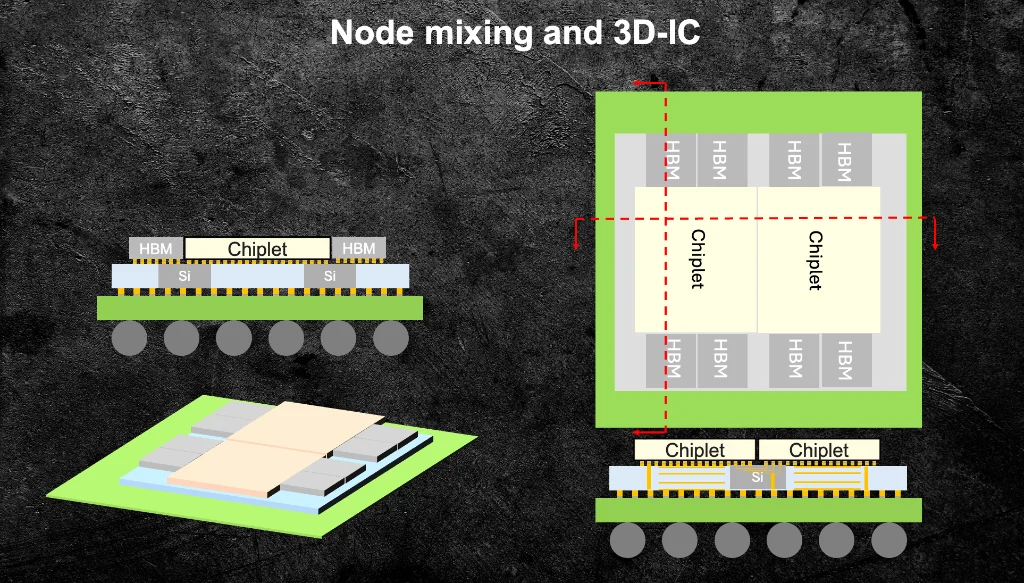
Slide 10: A representative chiplet floor plan integrating HBM, GPU, and CPU chiplets on a silicon interposer.
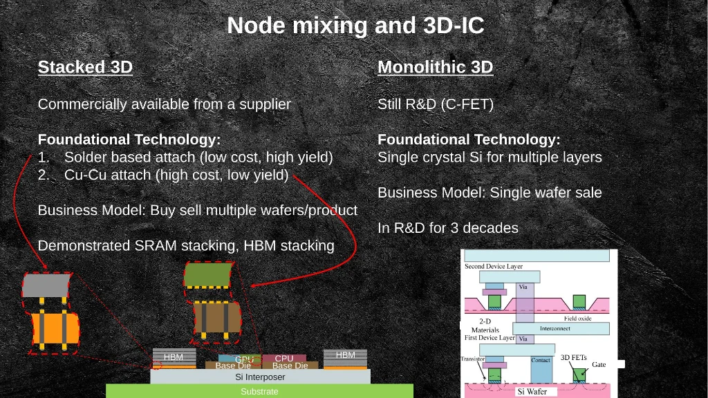
Slide 12: Stacked 3D (commercially available) vs monolithic 3D (still in R&D). The business model and foundational technology differ significantly.
Nasrullah distinguishes between stacked 3D — commercially available today, using solder or Cu-Cu attach — and monolithic 3D, which remains in R&D and requires single-crystal silicon for multiple active layers. Stacked 3D delivers yield improvements and better voltage-to-device matching today; monolithic 3D is a longer-horizon bet.
2. Low-Swing Die-to-Die I/O
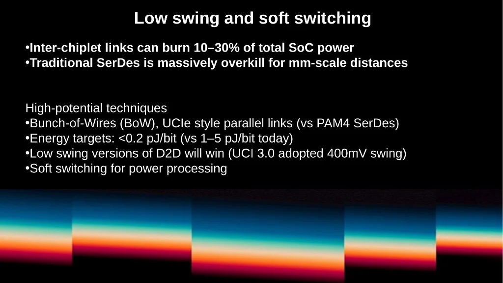
Slide 13: Inter-chiplet links can burn 10–30% of total SoC power. Low-swing techniques are the solution.
Traditional SerDes was designed for long-distance signaling over PCB traces and cables. Applying it to millimeter-scale die-to-die distances is, as Nasrullah puts it, "massively overkill." Inter-chiplet links currently burn 10–30% of total SoC power — a figure that is simply unacceptable at AI scale.
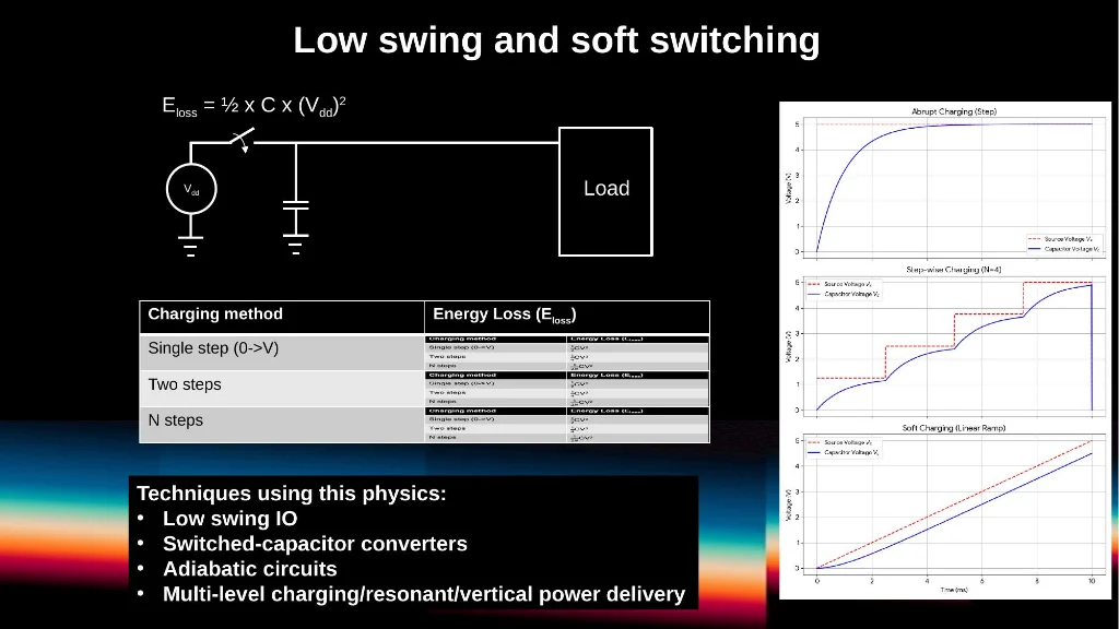
Slide 14: The physics of switching loss: Eloss = ½ × C × Vdd². Reducing the voltage swing has a quadratic effect on energy.
The physics are compelling: switching energy scales as ½ × C × Vdd². Cutting the voltage swing from 800mV to 400mV reduces switching loss by 75%. This is the driving force behind protocols like UCIe and HBM's steady migration to lower swing voltages.
IO Protocol | Vdd/Vddio (V) | IO Vswing (mV) | Data Width @ Freq | IO Energy (pJ/bit) |
|---|---|---|---|---|
HBM2 | 1.2 / 1.2 | 700–800 | 1024 @ ~2.5 Gbps | 1.5–2.5 |
HBM3 | 1.1 / 1.1 | 400–500 | 1024 @ ~6.4 Gbps | 0.8–1.3 |
HBM4 | <0.9 / 1.05 | 300–400 | 2048 @ 8 Gbps | 0.4–0.7 |
UCIe 1.0 | 0.75 / 0.9 | 600–800 | 64–256 @ 16 Gbps | 0.8–1.2 |
UCIe 2.0 | 0.70 / 0.8 | 400–600 | 128–512 @ 32 Gbps | 0.5–0.8 |
UCIe 3.0 | 0.65 / 0.7 | 250–400 | 256–1024 @ 64 Gbps | 0.25–0.4 |
3. Power Delivery Re-architecture
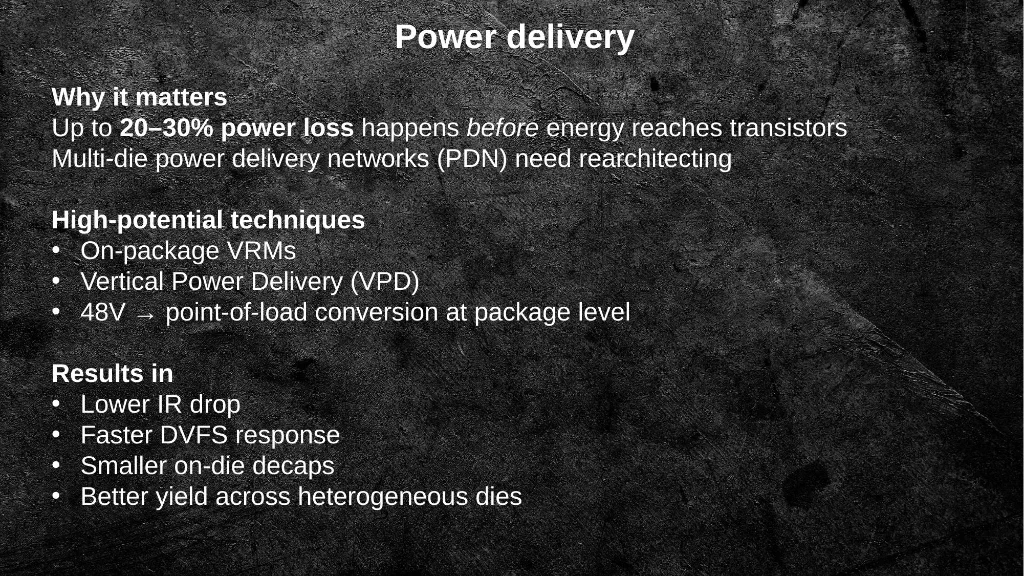
Slide 16: Up to 20–30% of system power is lost before it reaches the transistors. Power delivery network rearchitecting is essential.
A fact that surprises many outside the power delivery community: 20–30% of system power is lost before it ever reaches a transistor. This loss occurs in voltage conversion stages, PCB traces, package interconnects, and on-die distribution networks — and in a 1kW AI accelerator, that's 200–300W of pure waste heat.
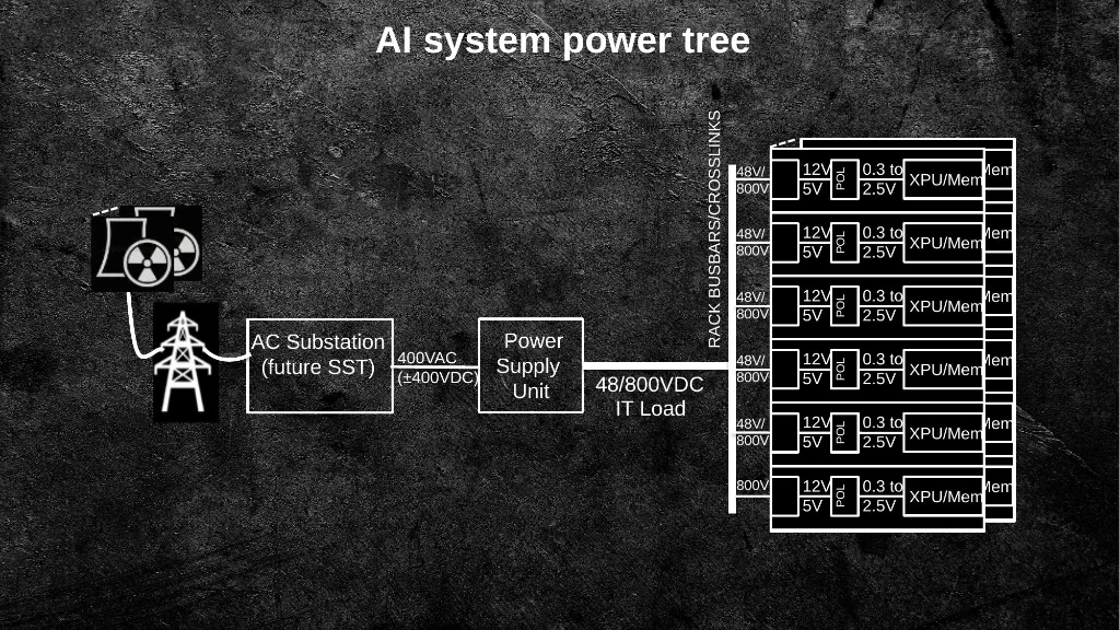
Slide 17: The AI system power tree: from 400VAC at the substation, through 800VDC distribution, to point-of-load conversion at the package.
The solution involves two architectural shifts:
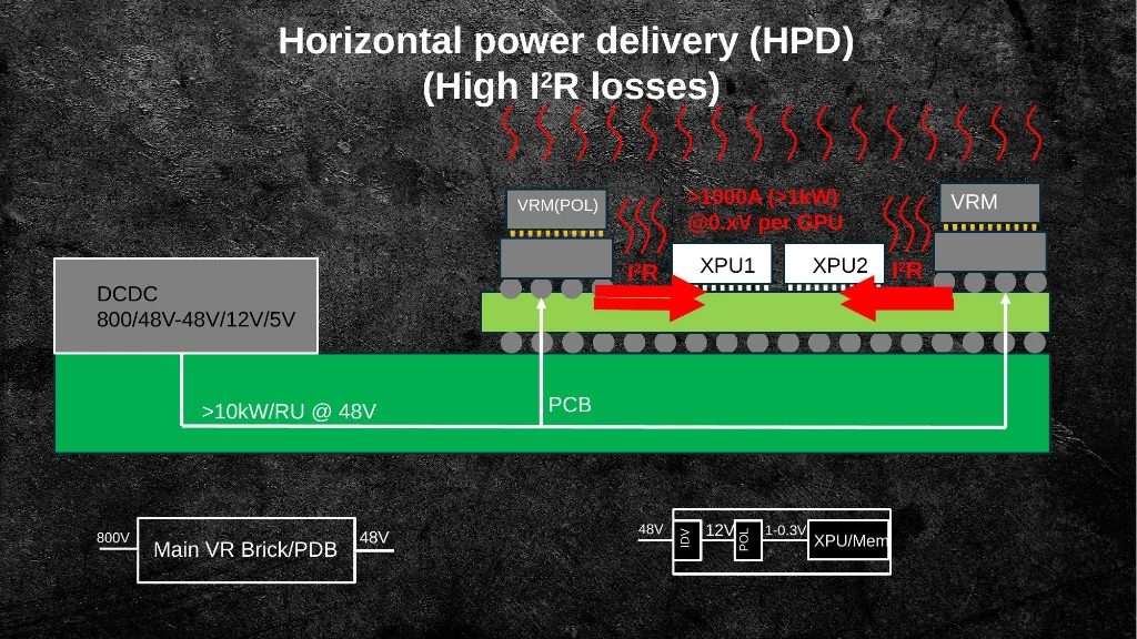
Slide 18: Traditional horizontal power delivery: VRMs on the PCB edge driving >1000A at sub-volt levels across long copper traces — high I²R losses.
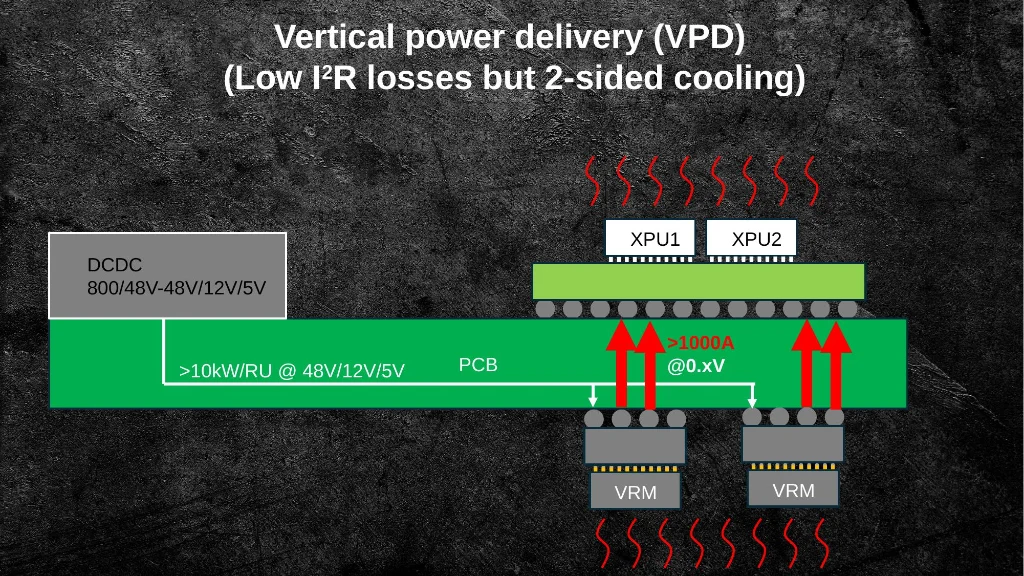
Slide 19: Vertical power delivery (VPD): VRMs mounted directly under the XPU, dramatically shortening the high-current path and cutting I²R losses.
Vertical Power Delivery (VPD) moves the voltage regulator module directly beneath the compute die, cutting the high-current path from centimeters to micrometers. The tradeoff is two-sided cooling, but the power efficiency gains — lower IR drop, faster DVFS response, smaller on-die decaps — are substantial for dense AI systems.
4. Memory Disaggregation and Near-Memory Compute
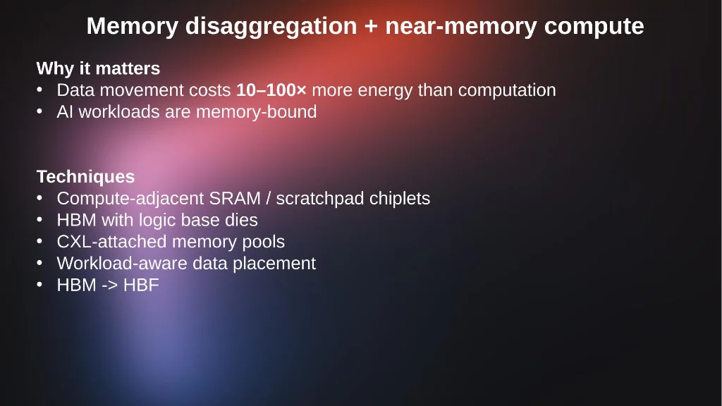
Slide 20: Data movement costs 10–100× more energy than computation itself — the strongest argument for near-memory compute architectures.
The final pillar addresses perhaps the deepest structural inefficiency in AI systems: data movement costs 10–100× more energy than computation. Moving data from DRAM to compute dies dominates the energy budget of AI inference, yet it's often treated as an afterthought in architecture discussions.
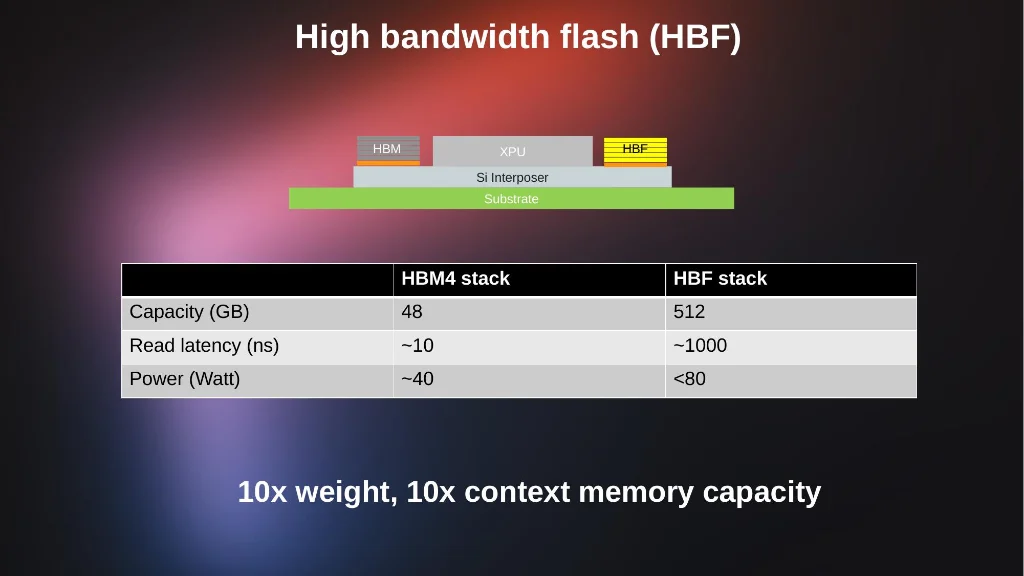
Slide 21: HBF vs HBM: 10× the capacity (512 GB vs 48 GB) for context-heavy AI workloads, at a fraction of the bandwidth cost per gigabyte.
Metric | HBM4 Stack | HBF Stack |
|---|---|---|
Capacity (GB) | 48 | 512 |
Read Latency (ns) | ~10 | ~1,000 |
Power (Watt) | ~40 | <80 |
High Bandwidth Flash (HBF) offers 10× the capacity of HBM4 per stack, enabling AI systems to hold dramatically larger context windows on-package. The latency penalty (~1µs vs ~10ns) is acceptable for prefetch-heavy workloads where the alternative is a round-trip to external DRAM or SSDs.
Call to Action: System-Level Co-Design
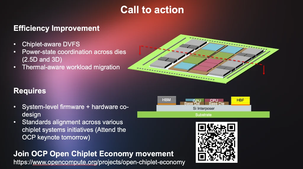
Slide 22: The call to action — chiplet-aware power management requires system firmware + hardware co-design, and standards alignment across chiplet ecosystem initiatives.
Nasrullah closes with a systems-thinking call to action. The four techniques above are not independent optimizations — they interact. Chiplet-aware Dynamic Voltage and Frequency Scaling (DVFS) requires power-state coordination across dies in both 2.5D and 3D configurations. Thermal-aware workload migration requires the firmware stack to see across die boundaries. None of this happens without standards alignment.
What Needs to Happen Next
Chiplet-aware DVFS: Power-state coordination across all dies in a 2.5D or 3D package.
Thermal-aware workload migration: System firmware that can see and respond to per-die thermal states.
System firmware + hardware co-design: The split between firmware and silicon must be rethought for multi-die systems.
Standards alignment: Initiatives like the OCP Open Chiplet Economy are critical for interoperability across vendors.
Summary
Dr. Nasrullah's talk at Chiplet Summit 2026 presents a clear and actionable framework for tackling AI's 10GW energy challenge through chiplet design. The four techniques — node mixing, low-swing D2D IO, vertical power delivery, and near-memory compute — are individually mature enough to deploy today and collectively powerful enough to bend the power curve meaningfully.
The deeper message is architectural: solving the 10GW challenge requires designing chiplet systems as integrated energy systems, not collections of optimized dies. The hardware, firmware, standards, and cooling layers must be co-designed from the start. For the semiconductor industry, this is both the hard part and the opportunity.
Explore the Open Chiplet Economy
Join the OCP initiative driving standards for chiplet interoperability, power management, and system-level co-design across the ecosystem.
Visit OCP Open Chiplet Economy →
Source: "Designing chiplets to accelerate AI: The 10GW challenge" — Dr. Jawad Nasrullah, Palo Alto Electron Inc. Presented at Chiplet Summit, February 18, 2026.
Published on chiplet.us · All slide images © Dr. Jawad Nasrullah / Palo Alto Electron Inc.