How modular silicon became inevitable in the age of AI
In engineering, terminology often attracts more debate than it deserves. Some engineers call them chiplets. Others prefer multi-die architectures, dielets or simply heterogeneous integration.
The name does not matter. What matters is a fundamental engineering rule: If a monolithic solution works, it should always be the first choice. But you will find that there is no easy escape from the chiplets when performance matters.
For decades, that was true. Monolithic integration worked because transistor scaling made it possible to pack ever-larger systems onto a single die. But two forces have fundamentally changed the equation:
• the slowing—and practical demise—of traditional transistor scaling
• an unprecedented explosion in global demand for computing
When those two trends intersect, a new architectural model becomes inevitable. That model is chipletization.
Before Chiplets Were Mainstream
Today, the word chiplet appears in nearly every semiconductor roadmap, conference, and investor presentation. But this was not the case when I started zGlue in 2014 in my Palo Alto garage along with Ming Zhang. At that time, most engineers had never heard the term chiplet. When the idea was explained—building systems from multiple small dies integrated in advanced packaging—the reaction was usually skepticism.
The industry was optimized for the System-on-Chip paradigm. Everything—from EDA tools to design methodologies to business models—assumed that a single company would design and manufacture a monolithic chip. The idea of building systems from reusable silicon building blocks felt foreign.
Yet the pressures on semiconductor design were already clear. Large monolithic dies were becoming harder to manufacture, more expensive to design, and increasingly inefficient when mixing different technologies such as logic, analog, RF, and memory.
The Origin of the Idea
The concept of chiplets did not emerge entirely from industry. We first heard the word chiplet from my professor at Stanford University, where the architectural idea of decomposing chips into smaller units had already been discussed academically. But academic ideas do not automatically become industry practice. At the time, there were essentially no startups developing chiplet platforms, and the semiconductor industry had no ecosystem around modular silicon.
The missing ingredient was productization.
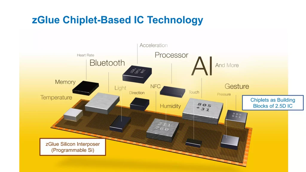
zGlue: Productizing the Chiplet Concept
zGlue attempted to turn the chiplet idea into a practical system platform. Instead of building complete SoCs, engineers could assemble systems from pre-existing silicon components integrated inside advanced packages.
The vision required several pieces:
• a silicon integration platform
• heterogeneous packaging technologies
• design tools capable of multi-die integration
• and most importantly, a marketplace of reusable chiplets
The goal was to make silicon development behave more like software development—modular, composable, and iterative. The concept was radical at the time, and we, at zGlue, even developed our own CAD tools as well. But the economic pressures on semiconductor design were already pointing in that direction.
The Industry Finally Moves
Over the next decade, the industry began to validate the chiplet model. Large processors adopted chiplet architectures. Advanced packaging technologies have matured a bit. High-bandwidth memory became tightly coupled with compute.
At the same time, computing demand accelerated dramatically due to AI, hyperscale infrastructure, and global data growth. The monolithic SoC model was no longer sufficient. Chiplets allowed systems to scale beyond the reticle limits and yield constraints of traditional semiconductor design.
Government Programs and Missed Opportunities
As chiplets gained attention, several government initiatives attempted to accelerate the technology. One example was the DARPA CHIPS program, which followed the emergence of chiplet platforms such as zGlue. The program focused heavily on large defense contractors and established semiconductor companies. While it helped bring visibility to heterogeneous integration, the program ultimately did not produce major commercial breakthroughs.
Later, the U.S. CHIPS and Science Act introduced initiatives such as the National Advanced Packaging Manufacturing Program (NAPMP) aimed at strengthening domestic packaging capabilities.
Unfortunately, many of these efforts were slowed by bureaucracy and structural inefficiencies. Meanwhile, real industry momentum was emerging through open collaboration.
The Open Chiplet Economy
In 2019, we participated heavily in launching the Open Chiplet Economy project within the Open Compute Project (OCP) Foundation. The initiative originally began under the name ODSA (Open Domain-Specific Architecture) and later evolved into the broader Open Chiplet Economy framework.
The objective was simple: Create the foundations for an open ecosystem of interoperable chiplets.
The project brought together hyperscalers, semiconductor companies, startups, and system architects to define practical standards enabling chiplet-based systems. Among the most important contributions were:
Bunch-of-Wires (BoW)
A lightweight die-to-die interface for efficient chiplet communication.CDXML (Chiplet Design Exchange Markup Language)
A framework for describing chiplets and enabling integration workflows.
These efforts helped ignite broader standardization across the industry and influenced emerging frameworks such as:
UCIe (Universal Chiplet Interconnect Express)
3D-Blox
Encouragingly, major companies—including Arm and many others—are now participating in the Open Chiplet Economy initiative to build interoperable chiplet-based systems.
Why Chiplets Disrupt the Traditional EDA Oligopoly
For decades, the semiconductor design ecosystem has been dominated by a small number of EDA vendors whose tools were optimized for monolithic SoC development. That model works well when a single company designs a single large chip.
Chiplets change that model fundamentally. Instead of designing a single monolithic system, engineers begin designing systems composed of multiple independently developed silicon components.
This introduces new design abstractions:
chiplet interoperability
system-level integration
packaging-aware architectures
reusable silicon building blocks
The design problem moves from transistor-level integration to system-level composition. This shift has two important consequences.
First, the traditional EDA flow—optimized for single-die design—does not naturally address the complexity of multi-die system architecture.
Second, chiplet ecosystems enable new entrants and new tools that operate at higher abstraction layers.
Just as cloud computing weakened the dominance of traditional enterprise infrastructure vendors, chiplets have the potential to disrupt traditional semiconductor design workflows. The companies that succeed in the chiplet era will not necessarily be those with the best transistor-level tools.
They will be the ones who enable system-level composability of silicon.
Manufacturing Reality and Global Challenges
Despite strong semiconductor innovation within the United States, the country still lacks a large-scale domestic capability for advanced packaging and chiplet manufacturing. We see a lot of slideware about advanced packaging capabilities, but the reality remains that today, there is still a single manufacturing source from Taiwan. Much of the practical implementation of chiplet technology, therefore, occurs in Taiwan and surrounding manufacturing ecosystems. This creates both opportunity and complexity. The manufacturing expertise exists, but collaboration across ecosystems introduces cultural and supply chain challenges. Nonetheless, global cooperation remains essential for the success of chiplet architectures.
Chiplets in the Age of AI
Artificial intelligence has dramatically increased the scale and complexity of computing systems. Modern AI infrastructure integrates:
massive compute arrays
high-bandwidth memory stacks
advanced networking fabrics
specialized accelerators
sophisticated power delivery systems
Building such systems as monolithic chips is increasingly impractical. Chiplets enable these architectures to scale efficiently. In many cases, the chip package itself is becoming the new system board.
Chiplets for the Long Tail of Computing
While hyperscale AI systems dominate headlines, some of the most important chiplet applications will emerge in:
robotics
automotive systems
industrial automation
edge devices
These markets require high-mix, low-volume silicon. Traditional SoC design economics struggle in these environments because the cost of designing a monolithic chip is too high for smaller production volumes. Chiplets provide a practical alternative. Reusable silicon components can be combined to build specialized systems without requiring a full custom SoC.
Timeline: The Evolution of Chiplets (2005–2030)
2005–2010 | Academic research begins exploring modular silicon architectures and heterogeneous integration concepts. |
2010 | The term chiplet appears in academic environments, including discussions within Stanford research circles. |
2014 | zGlue is founded in a Palo Alto garage and begins productizing the chiplet concept with a platform and marketplace approach. |
2016–2018 | Industry skepticism begins to shift as advanced packaging technologies progress and modular silicon architectures become viable. |
2019 | The Open Chiplet Economy initiative was launched within OCP (initially ODSA). |
2020–2022 | Standards and frameworks such as BoW and CDXML emerge, helping enable interoperable chiplet ecosystems. |
2022–2024 | Industry-wide standardization efforts accelerate with UCIe and system description frameworks like 3D-Blox. |
2025 and beyond |
|
The semiconductor industry transitions from monolithic chips to modular silicon systems.
Author
Jawad Nasrullah
Open Chiplet Economy Initiative – OCP
Chiplet.US