Yesterday, I visited the Computer History Museum after a while to spend some time reflecting on the giants whose shoulders today’s computing industry stands upon. Instead, I found myself staring at an unexpected mirror of the modern AI industry.
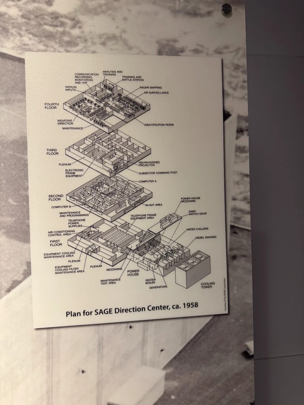
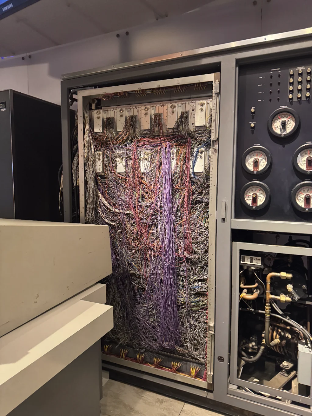
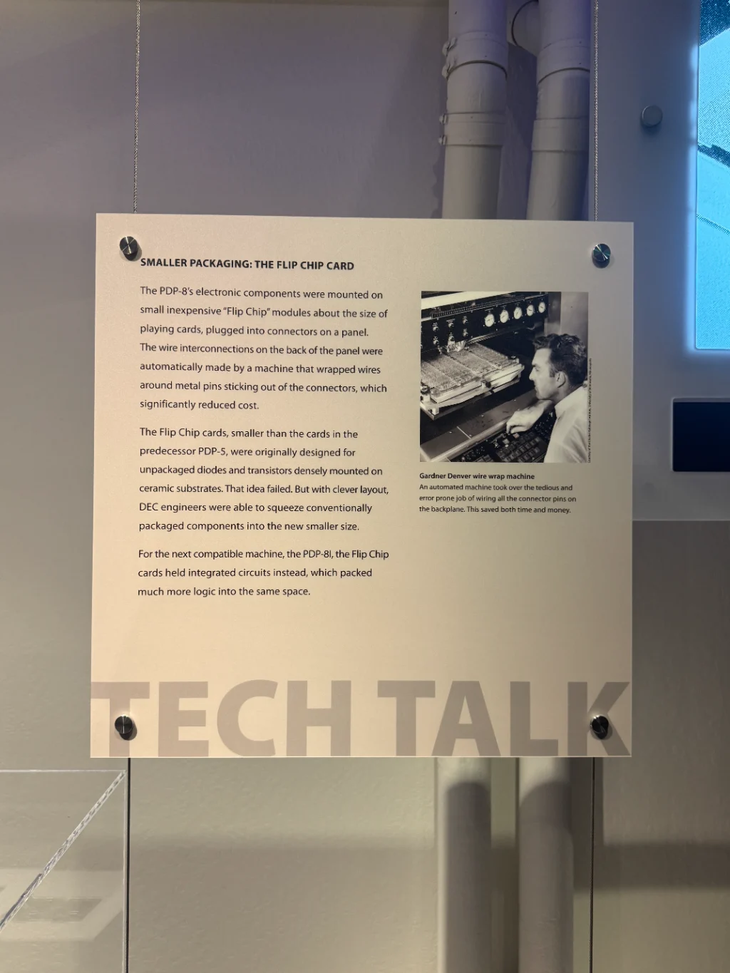
One exhibit showed the SAGE air-defense computer system (https://www.computerhistory.org/revolution/real-time-computing/6/122) from the 1950s — a massive computing installation spread across rooms and floors of a hardened building. Another showed flip-chip packaging innovations designed to reduce wiring complexity and improve integration density. At first glance, these systems appear primitive compared to modern AI accelerators and 3D ICs.
But the architectural problems were remarkably similar.
The industry today speaks about chiplets, 3D IC, advanced packaging, silicon interposers, HBM stacks, and heterogeneous integration. Yet looking at SAGE, it becomes clear that the computer industry is not solving a completely new problem. It is rediscovering an old one: Large-scale computing systems were and are fundamentally constrained by communication, power delivery, cooling, and physical integration.
The Computer Was Never Just the Chip
For decades, Moore’s Law allowed architects to think of computation primarily from the transistor outward for faster cores, denser logic, and smaller process nodes.
For many years, system-level inefficiencies could be masked by the next process node shrink. Faster transistors compensated for poor locality, inefficient communication, and excessive movement of power and data. That abstraction has now collapsed. Nanometers became “N” and angstroms became “A” as marketing shorthand, often discussed as if they represent direct physical dimensions. Meanwhile, the effective gate lengths of MOS transistors have remained in the tens-of-nanometers regime for quite some time, revealing how modern scaling is increasingly driven by architectural innovation, materials engineering, power delivery, and system-level integration rather than simple geometric shrinkage alone.
Modern AI systems are increasingly dominated by: memory movement, communication latency, rack power, cooling density, retimer power, substrate escape routing, and infrastructure-level efficiency.
In many cases, the “compute” itself is no longer the dominant challenge. The system is.
SAGE Was Essentially a Multi-Story 3D Computer
Looking at SAGE from a modern perspective, one striking realization emerges: SAGE was effectively a large-scale 3D integrated system. Not in silicon. But architecturally. Different floors of the building contained computer equipment, communications equipment, power systems, cooling infrastructure, operators, and interconnection pathways. The building itself became part of the computer architecture.
That sounds surprisingly familiar.
Modern 3D IC systems similarly stack compute dies, memory dies, power delivery structures, thermal extraction structures, communication fabrics, and control layers into tightly integrated vertical systems. The scale changed from rooms to microns.
But the architectural principle remained identical: Reduce communication distance to improve system performance.
“Advanced Packaging” Is Really System Architecture
The phrase "advanced packaging" feels increasingly incomplete because packaging is no longer a backend assembly step. A modern AI package determines memory bandwidth, thermal density, power integrity, latency, yield, manufacturability, and increasingly even software scheduling behavior.
The package has become part of the architecture itself. In some cases, it is becoming the architecture. This is why the industry’s terminology feels historically disconnected.
Many of the lithographic techniques used in silicon interposers or redistribution layers are not fundamentally new scientific breakthroughs. Semiconductor fabs mastered many of these dimensions decades ago.
The Dangerous Illusion of Silicon-Centric Design
Future systems must increasingly begin with:
workload movement,
topology,
memory locality,
rack-scale power,
cooling constraints,
communication fabrics,
deployment economics,
and infrastructure orchestration.
Only then can silicon be optimized correctly.
The Return of Physical Computing
For many years, software abstractions insulated the industry from physical reality.
Now AI is bringing physics back to the forefront: power, thermals, cooling, communication distance, and energy per bit moved.
It is the return of physical computing as the dominant systems problem. And history suggests this has happened before. SAGE engineers understood that the building itself was part of the computer. Modern AI infrastructure engineers are rediscovering that the package, board, rack, and data center must all become part of the computer architecture.
The Industry May Need a New System-Level Design Layer
The semiconductor industry historically separated:
chip design,
packaging,
board design,
thermal engineering,
power engineering,
and deployment infrastructure.
AI systems are collapsing those boundaries.
Future architectures may require continuous simulation across silicon, package, workload, power, thermal, and infrastructure behavior from the earliest stages of design. Not merely as backend verification. But as architecture itself.
The next generation of computing systems may ultimately be designed less like isolated chips and more like vertically integrated infrastructure systems — miniature SAGE buildings compressed into silicon-scale form factors.
And that may be the real meaning behind the awkward term “advanced packaging.”
Jawad Nasrullah (jawad@paloaltoelectron.com)
5/11/2026