🔥 The Industry Has Crossed a Line
We are no longer designing chips.
We are designing systems of chips.
AI has fundamentally broken the old model. What used to be a monolithic SoC problem is now a multi-die, multi-package, multi-system orchestration challenge.
The industry is not fully ready for what comes next.
🧠 AI Is Forcing a New Compute Architecture
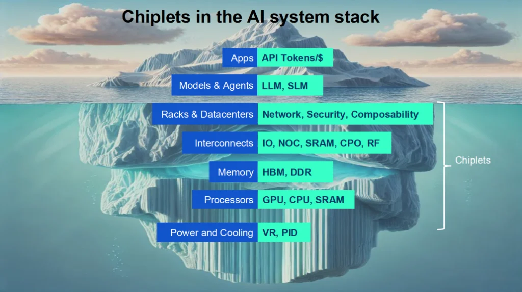
Modern AI systems demand:
Massive parallel computing (GPU, CPU, accelerators)
High-bandwidth memory (HBM, DDR)
Ultra-fast interconnects
Power and cooling at unprecedented density
The iceberg diagram shows something critical:
👉 Chiplets are embedded across every layer of the stack — from hardware to applications.
This is not packaging evolution.
This is a compute architecture revolution.
📦 From Silicon to Systems
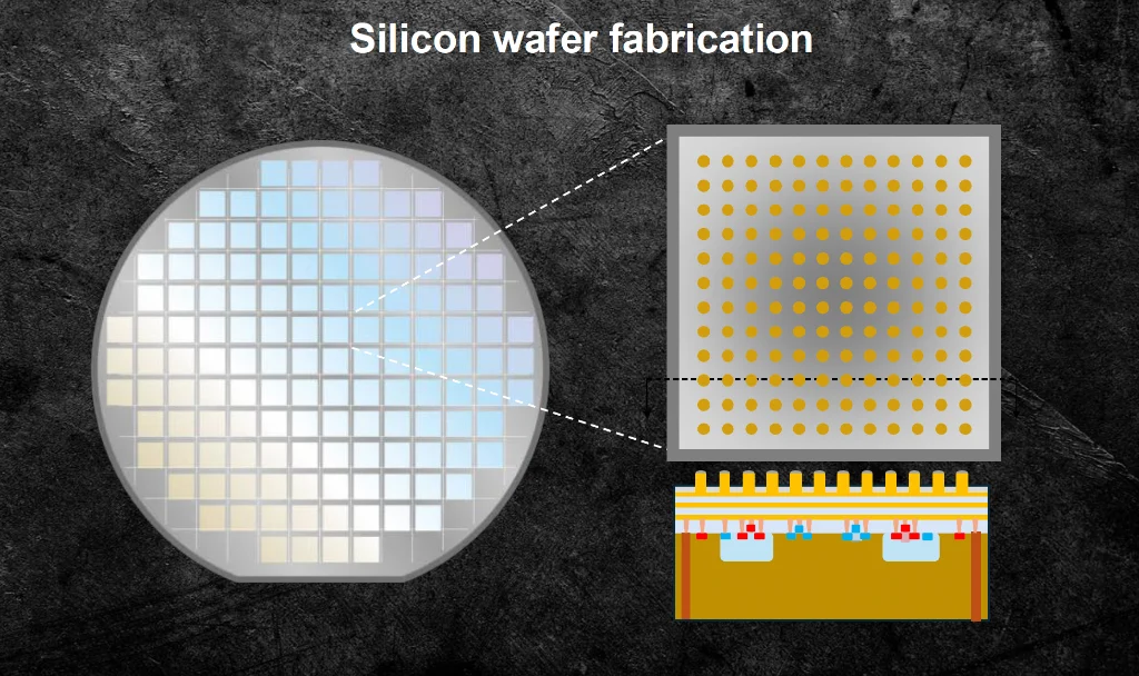
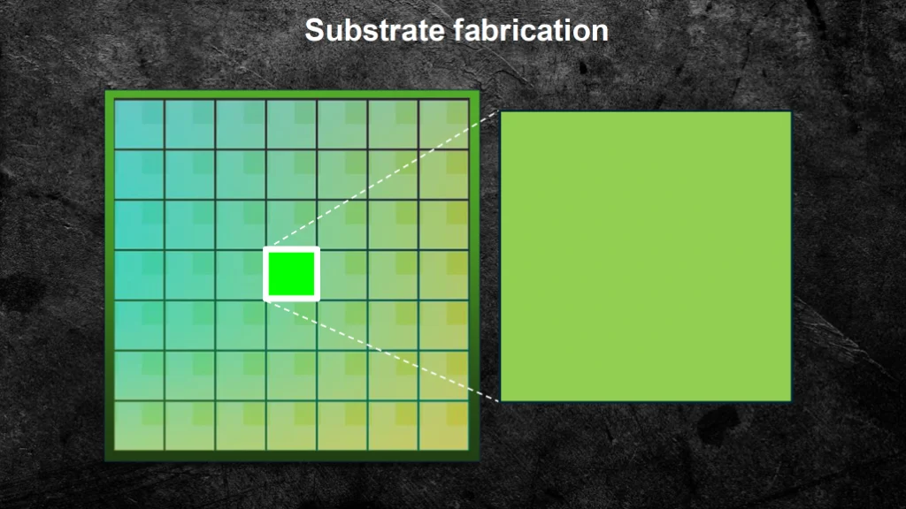
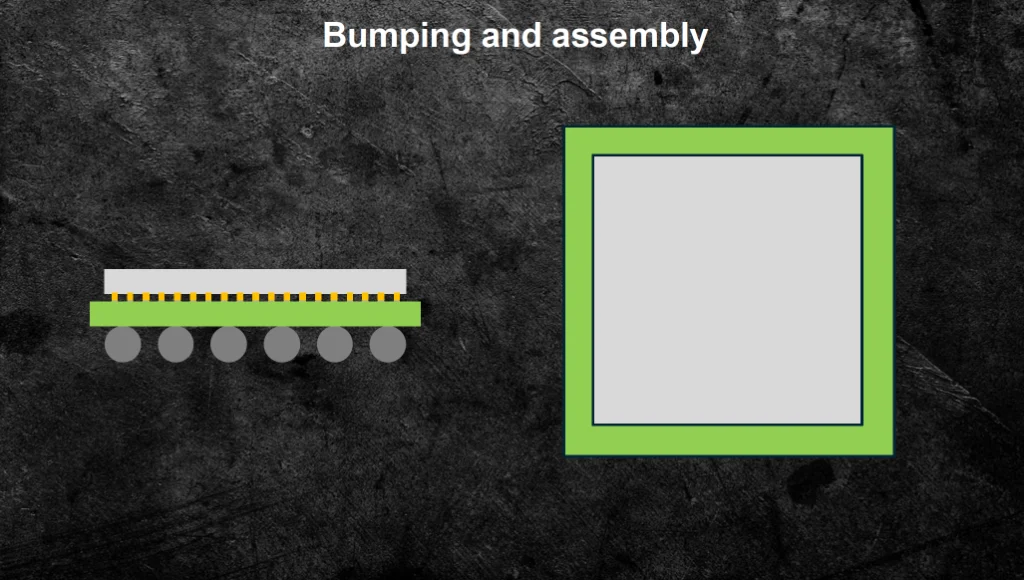
The traditional semiconductor flow:
Silicon wafer fabrication
Substrate fabrication
Bumping and assembly
But what used to be linear is now deeply coupled.
As shown across above figures, each stage now feeds directly into system-level decisions.
Packaging is no longer backend—it is part of architecture.
⚡ The Density Explosion
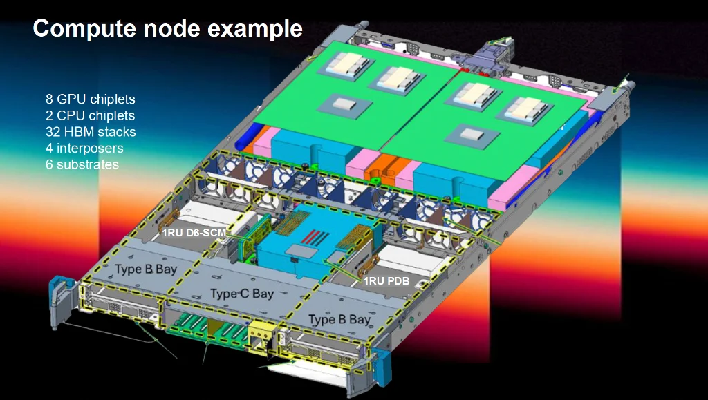
A single compute node today includes:
8 GPU chiplets
2 CPU chiplets
32 HBM stacks
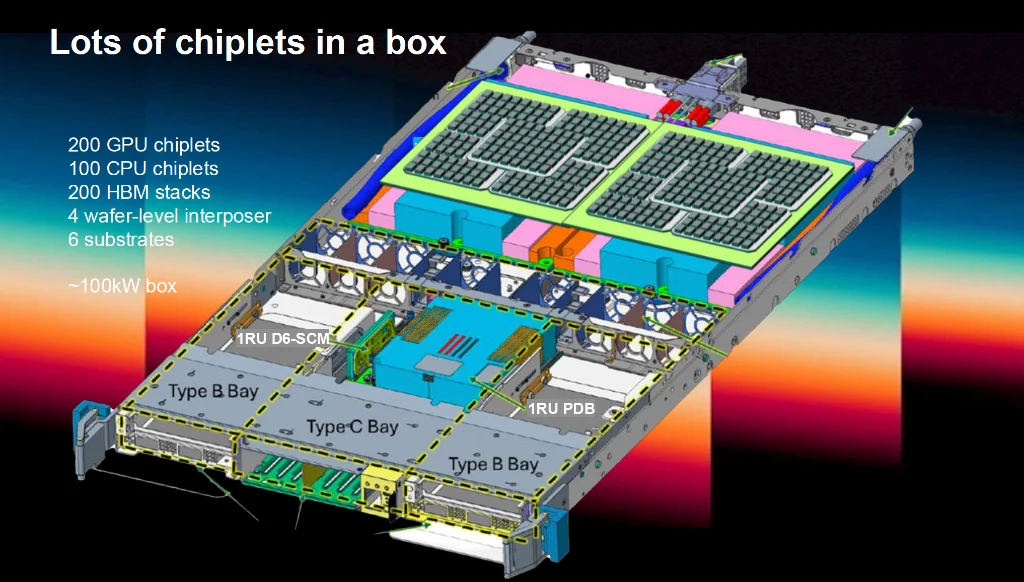
Now scale that:
200+ GPU chiplets
100+ CPU chiplets
~100kW system power
We are anticipating packing unprecedented compute into a single system.
The “chip” is no longer a chip.
It is a rack-scale system.
🌊 Cooling and Power: The Real Constraint
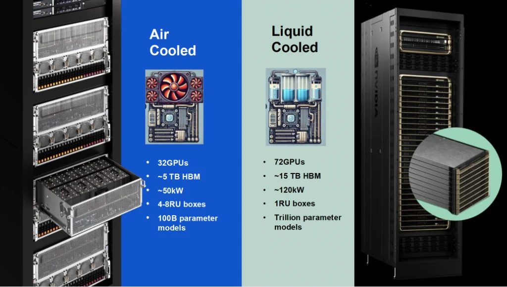
Air-cooled systems: ~50kW
Liquid-cooled systems: ~120kW+
This is not optional—it is physics.
Power and thermal are now first-class architecture constraints.
🧩 Two Models of Chiplet Integration
1. In-House Chiplets
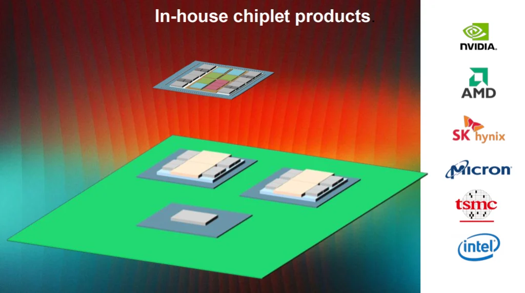
Vertically integrated
Highly optimized
Limited flexibility
Used by industry leaders controlling the full stack.
2. Chiplet Chassis (Emerging Model)
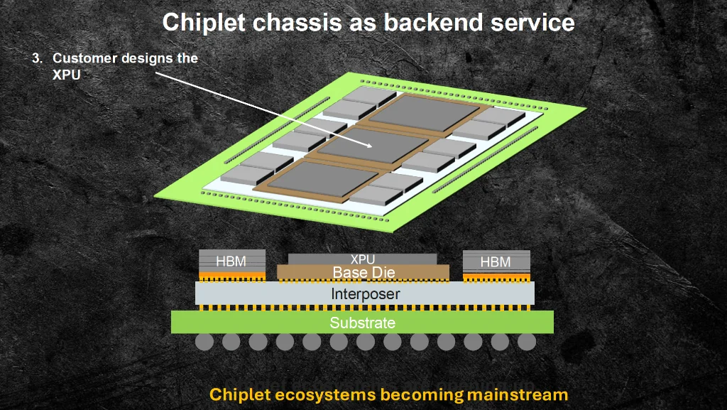
This is where things get interesting:
Base die with chiplet sockets
Reusable fabric
Plug-and-play compute
This is the beginning of hardware becoming modular and composable.
🌐 The Chiplet Ecosystem Is Forming
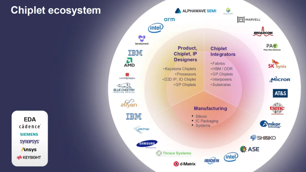
The ecosystem now spans:
Chiplet/IP designers
Integrators (interposers, fabrics)
Manufacturers (silicon, packaging)
EDA vendors
But:
The ecosystem exists… but it is not yet cohesive.
⚠️ The Real Problem: Design Complexity
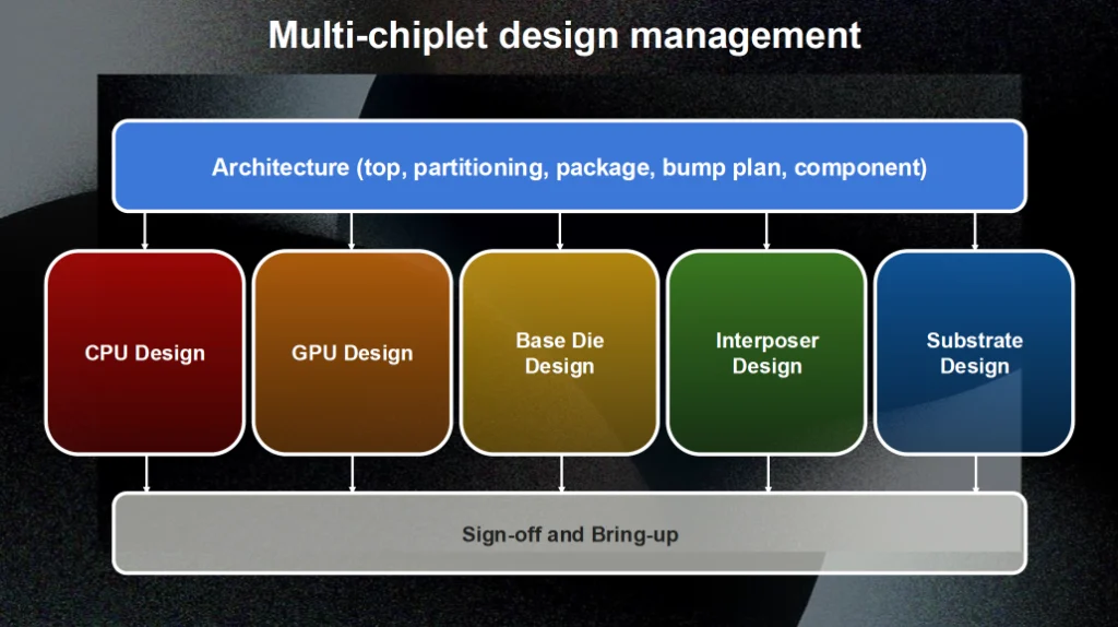
Designing chiplet systems requires:
Architecture partitioning
CPU/GPU/base die co-design
Interposer + substrate coordination
System-level signoff
The flow on page 21 makes it clear:
This is not chip design anymore.
This is system orchestration.
🔧 Critical Design Decisions
Technology Selection
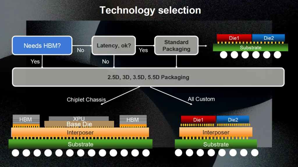
HBM or not?
Latency constraints
2.5D vs 3D vs advanced packaging
Package Architecture
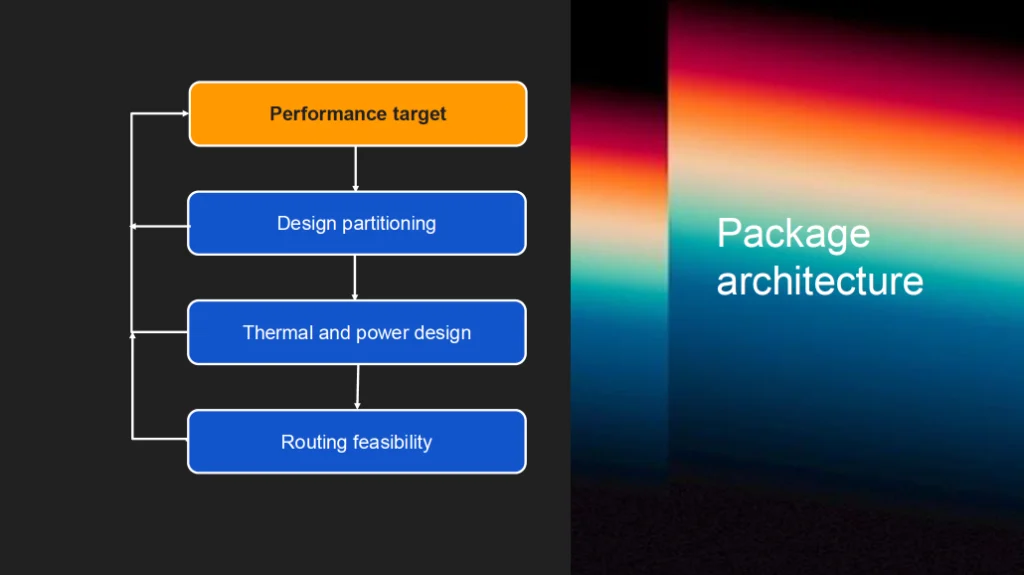
Partitioning
Thermal + power design
Routing feasibility
D2D Interconnect
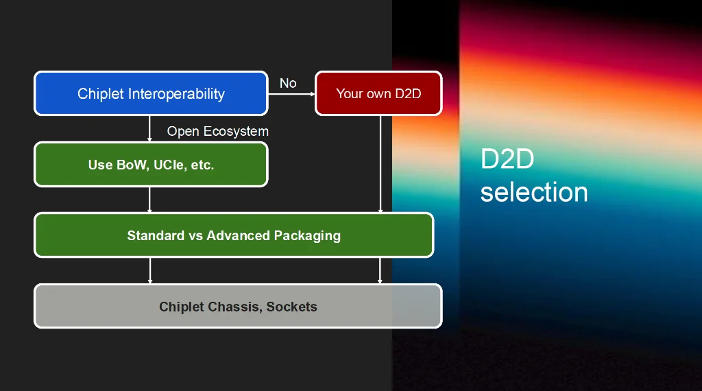
Open standards (BoW, UCIe)
Proprietary approaches
Ecosystem compatibility
🔮 Where This Is Going
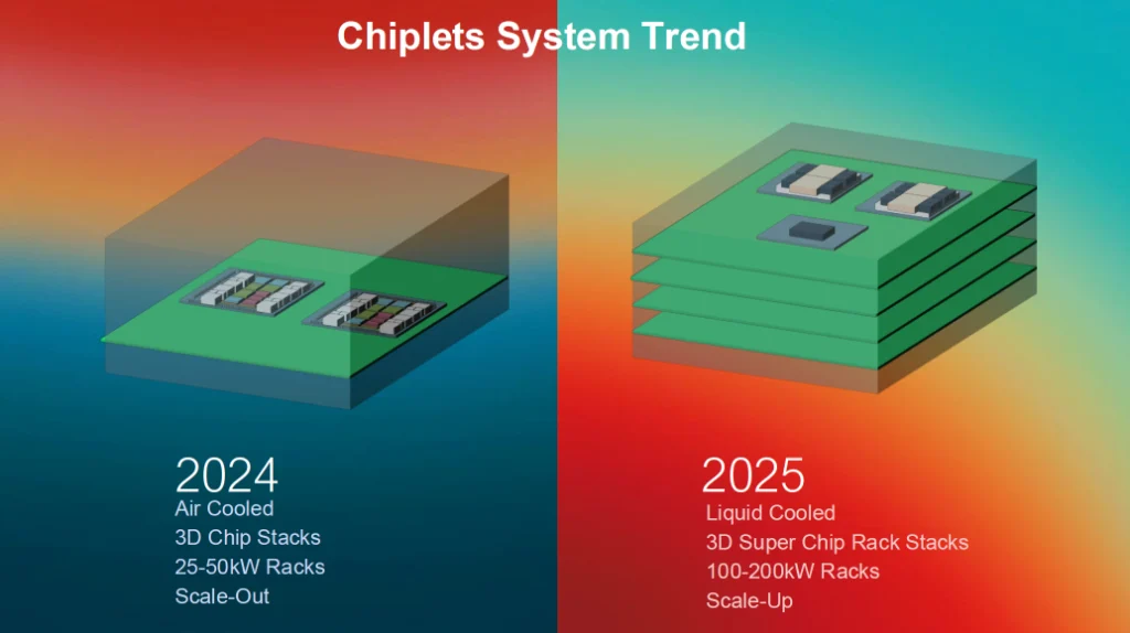
3D chip stacks → 3D system stacks
25–50kW → 100–200kW racks
Scale-out → scale-up
Interconnect density and system complexity will continue to explode.
⚡ The Hidden Lever: Power
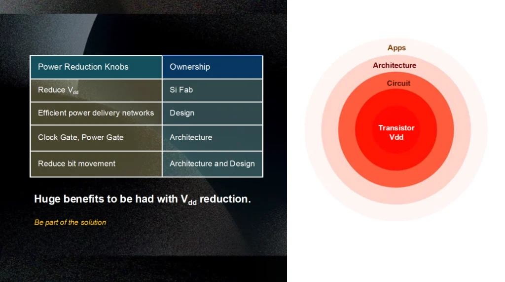
er Reduction Framework]
The most powerful lever:
👉 Reduce Vdd
But this requires coordination across:
Silicon (fab)
Circuit design
Architecture
Applications
Reducing data movement is as important as improving compute.
🧠 The Bigger Insight
Chiplets are evolving into:
Composable hardware
Platform-level systems
Modular infrastructure
Hardware is becoming programmable at the system level.
🚨 Call to Action
We have:
Incredible silicon innovation
Advanced packaging breakthroughs
A growing chiplet ecosystem
But we lack:
System-level abstraction
Integration frameworks
Scalable orchestration
The next wave of innovation will not come from better chips.
It will come from better system integration.
✍️ Final Thought
There is still a lot of chip designing to do.
But more importantly:
There is a lot of system designing to do.